| 8 - 0.1 small size | 1 - 5V DPDT relay AZ831-2C-5DSE | 2 - FT50-43, 10 bifilar turns, #22 |
| 1 - 47pf | 2 - 9-1/2 Turns, #24, 1/4" dia | 1 - BN-43-3312 balun, 2 - #20 teflon wires |
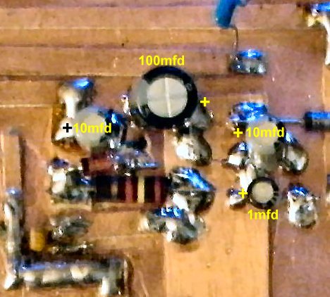
| 1 - 100mfd, 50V Electrolytic | 1 - 3-1/2 Turns, #24, 3/16" dia | 2 - TO-220 Mounting kits |
| 2 - 10mfd, 50V Electrolytic | 2 - IRF510 MOSFET | 1 - Heat sink compound |
| 1 - 1mfd, 50V Electrolytic | 1 - 2N3904 NPN transistor | 2 - 50 ohm small coax, 2' long |
| 1 - 2.2 mfd, 35V Tantalum | 2 - 10K trim pot | MRF 237 Amplifier Parts |
| 1 - 0.01 small size | 2 - 27 ohm, 1/4 W resistor | 1 - MRF 237 RF Transistor |
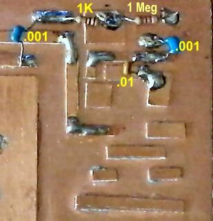
| 2 - 0.001 small size | 1 - 1K resistor | 3 - .01 |
| 1 - 1N4004 diode | 1 - 1 Meg resistor | 1 - FT37-43, 8 Turns, #24 wire 5-1/2" long |
| 2 - 1N4148 Diode | 2 - 300 ohm, 1/4 W, 3 dB pad | 1- FT37-43, 6 Turns, #24 wire 4-1/2" long |
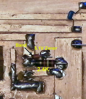
| 1 - 1N4733A, 5.1V, 1 W Zener | 1 - 18 ohm, 1/4 W, 3 dB pad | 1 - 27 mfd 50V Electrolytic |
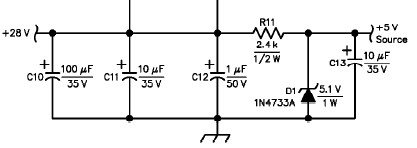
| 1 - 1N4746A, 18V, 1 W Zener | 1 - 2.4K 1/2W, or 2 - 4.8K 1/4W | 1 - 1/2" by 3" PCB |
| 1 - RF connector, RF out | 1 - FT50-43, 10 bifilar Turns, #24 | 1 - RF connector, VFO in |
|
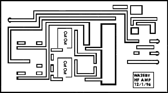
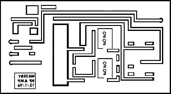
The mirrored layout below is the one that is used to make the Manhattan layout for building this version as shown in WA2EBY Manhattan Board Build. Note the different MOSFET Drain connections. |
|
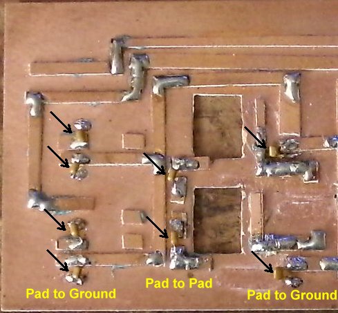
___8 - .1 capacitors, small size Notice that the left and right column of .1s go from a pad to ground. The center column of .1s go from a pad to a pad. Please Note: The small .01s are sensitive to heat, so check them after soldering to make sure a lead has not come off the cap. Note the top cap on the far left side. The white small strip on the bottom side of the cap could be a broken lead on the cap. Place the capacitor leads so they lay on the place to be soldered. Pushing a lead onto the pad with the soldering gun might break the lead from the cap. The most important place is on the left side of the board - the inputs to the MOSFETs. |
|
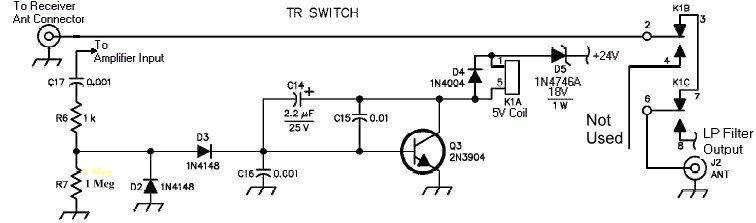
In Step 2 and Step 3 you will be building the TR switch. There are two modifications made in this section. First, the bottom lead of the .001 (C17) input capacitor for the RF switch is moved to the trace below the one shown in the standard layout from the ARRL. It is soldered to the trace that goes to the bottom terminal of the relay, as shown in the picture below. Second, that trace is cut (about 1/16" wide) after the .001 capacitor. If the trace is not cut, the output of the 1 Watt MRF237 amplifier will be connected to the receiver input when in receive mode decreasing receiver sensitivity. R7 can be raised to increase the sensitivity of the TR switch. This may be needed when driving a QRP transmitter when you have only the output of the VFO amplifiers to drive the TR switch. A 100K to 1 meg resistor can be used. When driving QRP transmitters with the BLT, this circuit is built dead bug style as a standalone board for TR switching. This can also be done with the WA2EBY to improve input/output isolation and placed at the output of the transmit LP filters. To provide for faster release of the relay (using high speed CW break-in and for working DX), C14, the 2.2mfm tantalum/electrolytic capacitor can be lowered to 1mfd. |
|
___2- .001 capacitors, small size ___1 - .01 capacitor ___1 - 1K resistor ___1 - 1 Meg resistor |
|
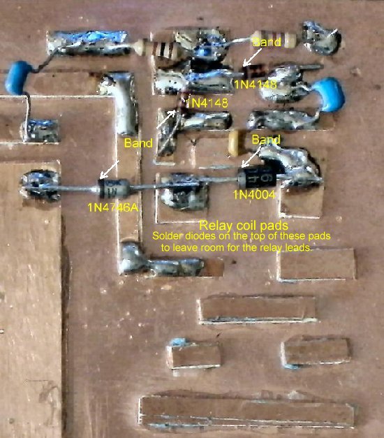
___2 - 1N4148 ___1 - 1N4004 ___1 - 1N4746A, 18 Volt, 1W Zener. Be sure to place the band of the diodes in the correct place. Solder the 1N4004 and the 1N4716A at the top of the pads (middle and right pads), as shown below. The relay coil leads will be soldered on the bottom of those pads. |
|
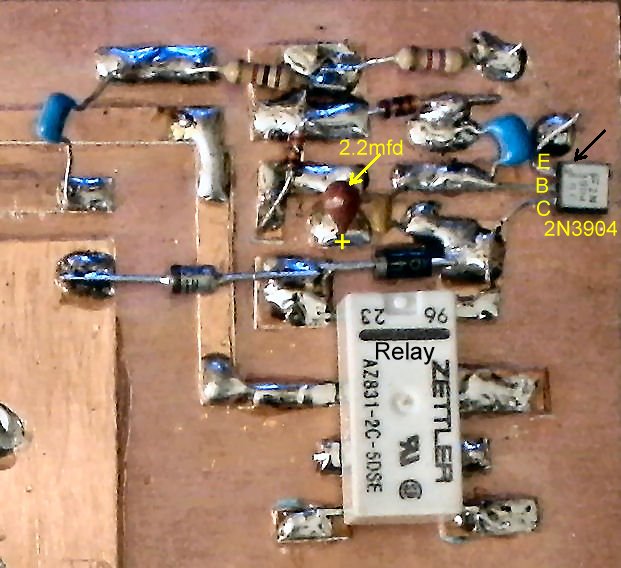
___1 - 2N3904 NPN transistor The "E" lead of the transistor is soldered to ground. ___1 - 2.2 mfd Tantalum capacitor, short lead is ground ___1 - 5V Zettler DPDT relay, AZ831-2C-5DSE The leads of the relay are bent straight out, laid on the pads and soldered. Solder one lead and check that the relay is oriented correctly - each lead is laying in the middle of its pad. |
|
The Zener function is unique. The Zener connects to the 24 Volt line and decreases the voltage to the relay according to the value of the Zener. In this case, the relay has a 5V coil, so 24V minus 18V (Zener value) equals 6 Volts (measured 5.5V) for the relay coil. |
|
___1 - 2.4K, 1/2 W or 2 - 4.8K, 1/4 W resistor ___1 - 1N4733A, 5.1V, 1 W Zener |
|
___1 - 100 mfd, 50V Electrolytic ___2 - 10 mfd, 50V Electrolytic ___1 - 1 mfd, 50V Electrolytic |
|
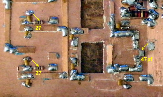
___2 - 27 ohm, 1/4 W resistor. NOTE! Check these resistors if you blow one or both of the MOSFETs. They will look burned and may not be broken apart. They usually short when burned which can contribute to another blown MOSFET. ___1 - 47pf capacitor |
|
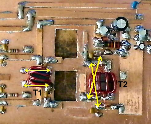
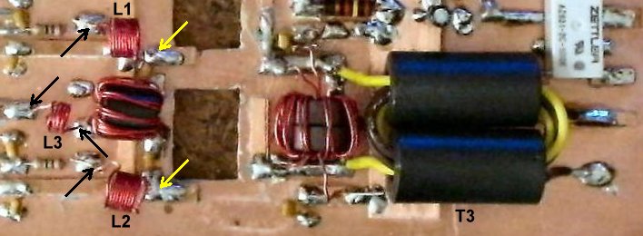
___1 - FT50-43 ferrite core, 10 bifilar turns, 2 - #24 wire 8-1/2" long, for T1 input transformer ___2 - FT50-43 ferrite cores stacked with 10 bifilar turns, 2 - #22 Wire 13" long, for T2 phase power transformer, The cores shown below were some surplus cores I had on hand during the build of this amp. Both are -43 material, larger than the ones specified in the original article. They worked well even though oversized. The cores in the kit are the specified cores, FT50-43. The yellow lines represent each wire winding and where they are soldered. Notice the T1 input transformer windings go straight across and T2 windings cross over. NOTE! It is important to get the T2 connections correct as a mistake will blow a MOSFET. You have to check if the ends of the wires are correct on T2 before you solder them to the board. After they are soldered, since one on each side goes to B+, you can't check them after they are soldered onto the PCB. |
|
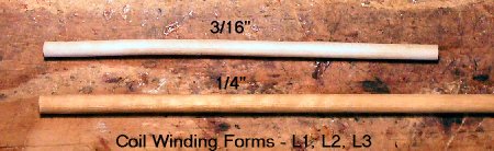
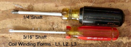
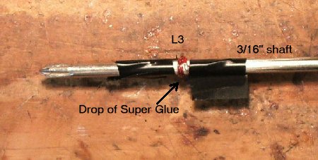
There are two coil winding forms you can use to make L1, L2, and L3. Dowel sticks from the hardware store or screwdrivers with shanks the correct size, one 1/4" and one 3/16". ___1 - L3, 3-1/2 Turns on a 3/16" form with #24 enameled wire 3-3/4" long.___2 - L1, L2 9-1/2 Turns on a 1/4" form with #24 wire 9-1/4" long |
|
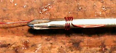
The winding of L3 is shown below. I used electrical black tape as shown in the second picture and then placed a small drop of Super Glue on the windings to hold the coil together. Don't let it dry overnight or it will be stuck to the screwdriver. Remove after about an hour and it will slip right off. |
|
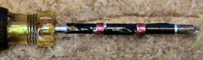
The winding of L1 and L2 is shown below. The super glue has been put on the windings. |
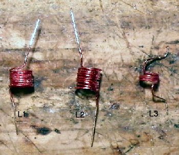
| The completed coils are shown in the picture below. |
|
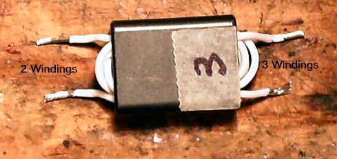
___1 - BN-43-3312 balun core, Pri 2 Turns, Sec 3 Turns. Wind Pri winding first, then wind Sec winding. Make sure you mark one of the windings on the core so you know which end is the 2 turn and 3 turn side. Using the same color wire for both windings makes it difficult to see what you did after winding the transformer. ___2 - Pieces of #20 teflon coated wire. 2 turn winding 6-1/2" long, 3 turn winding 9" long |
|
Solder the coils L1, L2, L3 and transformer T3 to the PCB. T3 below uses two larger cores (some -43 surplus cores on hand) and larger Teflon wire. Both the original T3 and this one had the same output. |
|
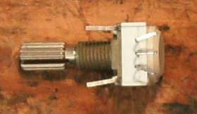
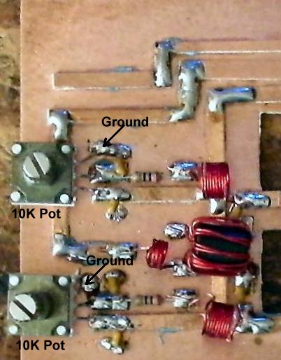
___2 - 10K Trim pots In the picture above notice how the outside leads are spread apart slightly to fit the traces when they are soldered to the board. |
|
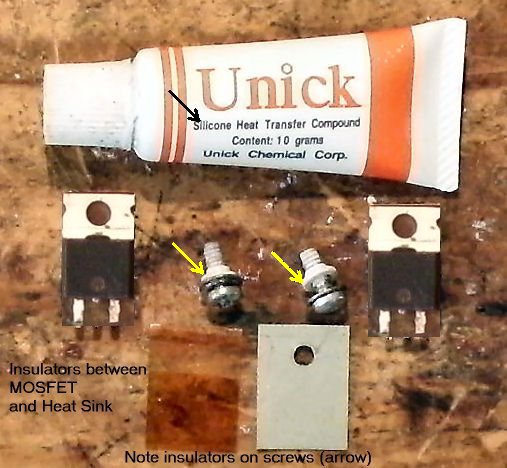
Shown below is what is needed to mount the MOSFETs. The MOSFET leads are cut short as shown below, the middle lead (drain) is cut off. Some Silicon Heat Treatment Compound is used (depending on type of insulator), and the MOSFET tab is isolated from ground (the tab is hot with 24 volts and the RF Output). |
|
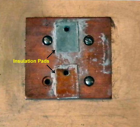
Shown are two different types of insulators. A TO-220 mounting kit can be purchase from DigiKey (and other companies) or the insulators can be robbed from discarded computer power supplies or audio amplifiers that use TO-220 output transistors. You will need the insulator and the insulating washer that will be on the mounting screw. The insulator shown on the left is made of mica and needs Silicon Heat Transfer Compound. The grey colored one is thicker and more durable and does not need the Silicon. Both work well in this amplifier. The screw used to mount the MOSFETs to the heat sink must have an insulating washer to keep the metal of the screw from touching the MOSFET tab. Note the arrow pointing to the insulating washer. It has a smaller section that goes inside the hole of the MOSFET tab to prevent a connection. The Drain connector lugs are standard ground lugs that have been modified to connect the heat sink (connected to the Drain) to the trace on the board. The center mounting holes are enlarged with a 1/8" drill so the insulating washer can fit and the right side of the lug (as shown below) is cut enough to allow the hole to fit correctly on the MOSFET. You may also have to cut the other side also. The easiest way is to hold the lug with pliers (or snap pliers) and rub the edge against a file. 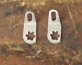 The following picture shows how the drain lug is mounted along with the spacer and screw. Note that the insulating spacer is above the Drain tab isolating both the MOSFET heat sink and the Drain lug from the screw. After finishing the mounting, make sure to check with a DVM that the Drain tab is not grounded to the heat sink. 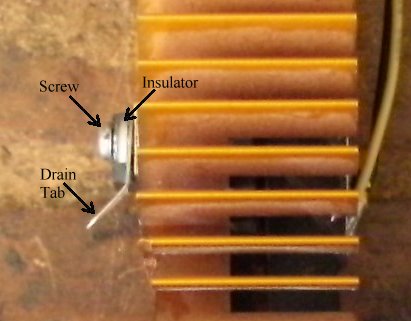 Bend the lug horizontal so that it can be soldered to the Drain trace on the PCB board. 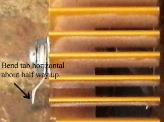 A 3/16" long 4-40 screw is used to mount the MOSFETs. After the MOSFETs are soldered to the board, the board is laid down on the heat sink and a pointed punch is used to mark the center of the hole on the heat sink. There are two ways to mount the MOSFETs to the heat sink. First, with heat sinks that have an thin base area underneath the MOSFETs, drill and mount a screw/nut. A 1/8" hole is drilled through the heat sink and is secured with a 4-40 screw, insulating washer, drain connection lug, and a nut underneath the heat sink. Second, heatsinks that have a very thick base area underneath the MOSFETs, a drill and tap are used to mount the MOSFETs. Use a 3/32" drill to make the holes and make the threads with a 4-40 tap and tool. A 1/4" or 3/16" long 4-40 inch screw (with insulating washer) will probably work best in this case. In the picture below, a copper heat sink from a computer processor was mounted onto an 8-1/2" by 8-1/2" aluminum plate. This heat sink has worked well. The copper plate was thick enough to drill and tap for 4-40 screws. |
|
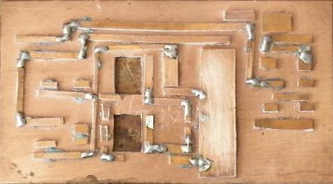
After soldering the Drain lug to the trace, use a DVM in short check mode, with tone indicating a short, between the tab and ground. Should be no tone (no continuity). To double check the MOSFET, check between the gate (left pin) and drain to make sure there is no continuity (no tone). You should always do this when replacing a blown MOSFET. Also check the 27 ohm bias resistor especially if it shows a dark color. The completed board. |
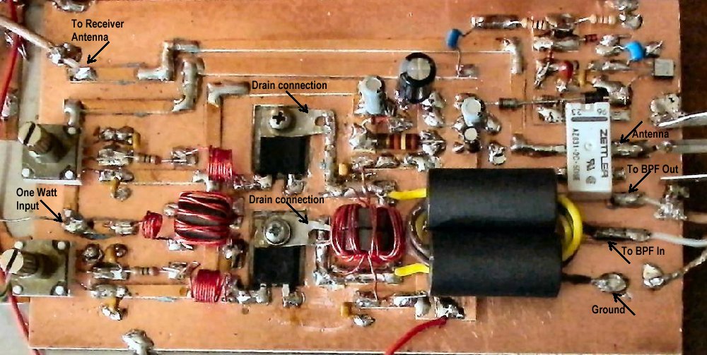
Connections to the board.The BLT does not do switching from receive to transmit at the Antenna terminal. The transmit signal is taken off the end of the VFO amplifier chain, therefore, connections are different from the original design. The Receiver connection of the transmitter goes to the Antenna input of the BLT. The VFO output goes to a MRF237 amplifier (2 Watt Output), a 3 dB Pad, then to the input of the WA2EBY amplifier. The output connections are as designed. The output of the WA2EBY amplifier goes to the input of the LowPass Filters, then the output of the LowPass Filters goes to the TR relay. The top connection of the relay contacts is the RF Output which goes to the outdoor antenna. |
Bias AdjustmentThe articles for the amplifier can be found with the following links: Part 1: A Broadband HF Amplifier Using Low-Cost Power MOSFETsPart 2: A Broadband HF Amplifier Using Low-Cost Power MOSFETs |
|
Picture shows completed dead bug build of the MRF237 2 Watt amplifier. |
|
First step is to use a piece of fine emory cloth (or sandpaper) to roughen up the side and bottom edge of a small area on the MRF237 so it will take solder easily. The whole bottom of the MRF237 does not need to be soldered to the board. Only a small, but good solder joint, will be needed to be effective in grounding the emitter (which is the case) and providing a good heat sink. |
| Notice the tab facing toward the front of the pliers. |
| A small amount of solder on the bottom edge of the MRF237. It shouldn't take too long to get the solder to take, in fact, the transistor should barely get warm. It is now ready to solder to the PCB. |
|
I cut this piece from the corner of the PCB that already had a hole that could be used for mounting the board. |
|
Orient the MRF237 so the B connection is on the input side of the board and the C connection is on the output side of the board. First solder a blob on the PCB and then put the MRF237 against it and melt the solder together between the PCB and the MRF237. |
|
___2 - Standoff resistors, value greater than 5 megohm ___2 - .01 mfd ___1 - 27 mfd, 35 V, Electrolytic ___2 - 300 ohm, 1/4 Watt, 3dB Pad ___1 - 18 ohm, 1/4 Watt, 3dB Pad |
|
___1 - .01 mfd ___1 - FT37-43 8 Turns, #24 5-1/2" long ___1 - FT37-43 6 Turns, #24 4-1/2" long |
|
The reason for not soldering B and C on the MRF237 is the short lead length of the pins. After the other parts are soldered, they are supported so that they can be carefully placed at the pins for soldering so that no shorts occur on the case of the transistor. |
|
Solder the B and C pins on the MRF237 |
|
The only thing left is to determine if you want to add a connector to the input side of the amp. The input is connected to the output relay of the VFO amplifiers of the SLR. The output side is connected directly to the input trace (where L3 is soldered) of the WA2EBY. |
|
A crude, but effective, RF connector (RCA phono) added to the amplifier. Ready to implement in front of the WA2EBY amplifier. Cut a small piece of PCB the width of the amp PCB and about 1" tall. Drill a 1/4" hole for the female connector. Then use at least one side support to hold the small piece of PCB steady. Without the side support it will bend easily and eventually break off. Solder at the edges at enough places to hold the pieces securely. |