| 8 - 0.1 small size | 1 - 5V DPDT relay AZ831-2C-5DSE | 2 - FT50-43, 10 bifilar turns, #22 |
| 1 - 47pf | 2 - 9-1/2 Turns, #24, 1/4" dia | 1 - BN-43-3312 balun, 2 - #20 teflon wires |
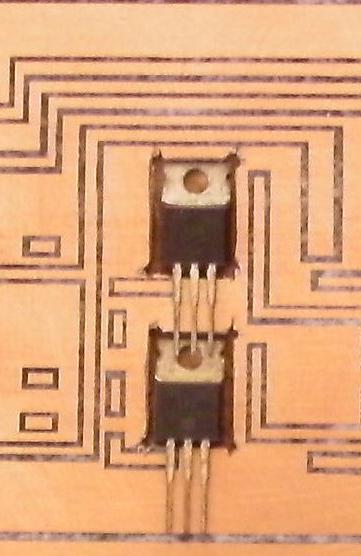
| 1 - 100mfd, 50V Electrolytic | 1 - 3-1/2 Turns, #24, 3/16" dia | 2 - TO-220 Mounting kits |
| 2 - 10mfd, 50V Electrolytic | 2 - IRF510 MOSFET | 1 - Heat sink compound |
| 1 - 1mfd, 50V Electrolytic | 1 - 2N3904 NPN transistor | 2 - 50 ohm small coax, 2' long |
| 1 - 2.2 mfd, 35V Tantalum | 2 - 10K trim pot | MRF 237 Amplifier Parts |
| 1 - 0.01 small size | 2 - 27 ohm, 1/4 W resistor | 1 - MRF 237 RF Transistor |
| 2 - 0.001 small size | 1 - 1K resistor | 3 - .01 |
| 1 - 1N4004 diode | 1 - 4.7K resistor | 1 - FT37-43, 8 Turns, #24 wire 5-1/2" long |
| 2 - 1N4148 Diode | 2 - 300 ohm, 1/4 W, 3 dB pad | 1- FT37-43, 6 Turns, #24 wire 4-1/2" long |
| 1 - 1N5338, 5.1V, 1 W Zener | 1 - 18 ohm, 1/4 W, 3 dB pad | 1 - 27 mfd 50V Electrolytic |
| 1 - 1N4689, 5.1V, .5 W Zener | 1 - 2.4K 1/2W, or 2 - 4.8K 1/4W | 1 - 1/2" by 3" PCB |
| 1 - RF connector, RF out | 1 - FT50-43, 10 bifilar Turns, #24 | 1 - RF connector, VFO in |
|
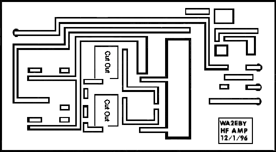
Note that the layout below is the advanced layout. This board uses a different connection to the MOSFET drain to enhance stability. |
|
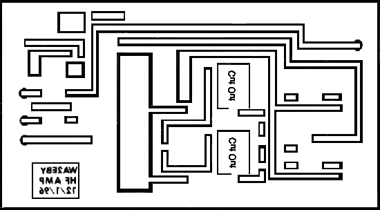
The following layouts are downloaded and printed to the following sizes: The default for most picture programs will be 72 pixels per inch, be sure to change to 200 pixels per inch if you have to use pixels. You can right click the following layouts and "Save Image As" or "Copy Image" to download (put in Clipboard) and open in Paint Shop Pro, LView Pro, Jasc Paint Shop Pro, IrfanView (Free). IrfanView has a 32 bit and 64 bit version for everything from Win 98, XP, up to Win 10. With IrfanView, do Edit/Paste, go to Image, Resize/Resample and Click on "Set new size", and enter the size in inches. The layouts can be properly sized with any of the above programs. The bottom one (mirrored) is the one used to produce the Manhattan style layout. |
|
The folowing is a piece of single sided 1/16" PCB board. On thicker PCB boards (1/16") the MOSFET leads will have to be bent up slightly and checked to make sure they do not touch the ground around their hole. Clean with 440 grit sandpaper and then wash it with soap and water, then dry. |

|
Use a laser printer to copy the mirrored layout above on some glossy paper or paper made for tranferring laser print to PCB board material. I use HammerMill Office One, Business Gloss. Size it to 5.75" width by 3.18" height. Pixel size is 1725 width by 953 height. For this application it is not very critical because a printed circuit board is not being made. It is simply a picture on the board to guide one for installing traces and a few rectangles. |
|
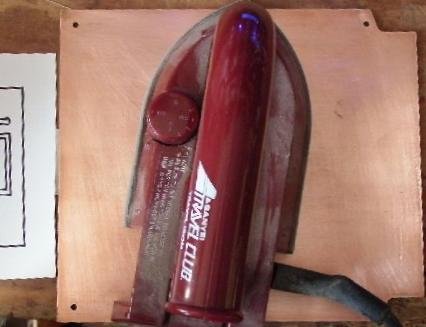
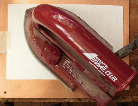
Use any iron for clothes at medium to hot heat and pre-heat the PCB board first. Getting the PCB hot first will lessen the time you have to press on the layout to get it transferred to the PCB. |
|
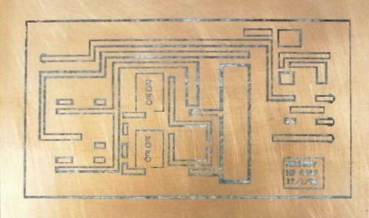
You can tell when it is finished by gently lifting a corner of the paper and see if it is stuck to the PCB. Fill a sink with about 3 to 5 inches of warm water, let the board cool for a while, then lay it gently into the water. The water will soak into the paper and make it very soft and piable so it will come off the board easily. Let it soak for 15 to 30 minutes and check the paper. Very gently lift it and see if it comes off the board. On the traces of the upper board it may still be stuck, but if the rest of it is coming off, you can go ahead and pull it from the areas of dense traces. Then use your fingers to roll off the remaining paper. The result will look like the following picture. If it is messed up so bad it can't be used, sandpaper the PCB again, and try again. You don't need a perfect print, just one that shows where to glue the traces and rectangles. |
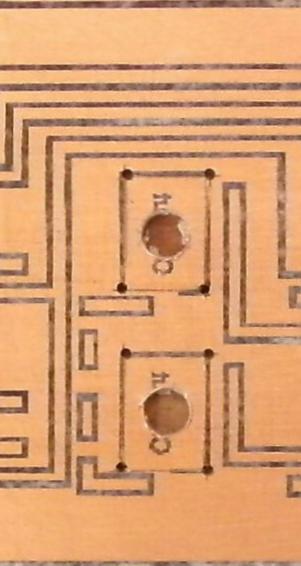
Cutting the MOSFET HolesShown below is how the MOSFET holes are cut out of the paper layout and then the edges of the holes are marked on the PCB. A utility knife is used and deep cuts are made through the copper layer and bottom side of the PCB.   Use a 1/16" drill and drill a hole at each corner of the holes. Then with a 1/8" drill bit, drill a hole in the middle of the MOSFET rectangle and then follow up with a 1/4" or 3/8" drill bit.
|
|
With the utility knife and a ruler, cut lines through the Copper layer and bottom side as shown above and below as deep as you can. Use the 1/16" holes as guides with a ruler to cut the lines on all four sides. I wasn't perfect with the cuts below.  With a Jig Saw and a narrow blade, or if the center hole was drilled with a 3/8" drill, a regular blade, cut from the center to each corner hole. If you don't have a Jig Saw, use a small wire cutter and cut from center hole to the corner holes. 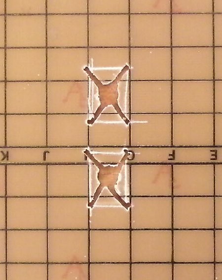 Use a needle nosed plier or wire cutter to break off the side pieces. If they don't break easily, cut into the side lines deeper until they do. Use the utility knife or a file to clean up the sides. Check the fit of the MOSFETs after finishing work on the hole.
|
|
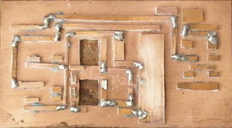
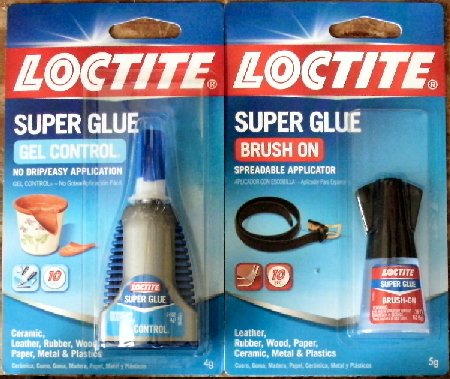
Use Super Glue to glue the traces/pads to the PCB. Super Glue Gel Control is the preferred glue. The Super Glue Brush On was used but it didn't lay enough glue on the traces/pads to make them stick well to the PCB. The Gel leaves a good drop on the traces/pads and sticks very well to the PCB. |
|
|
|
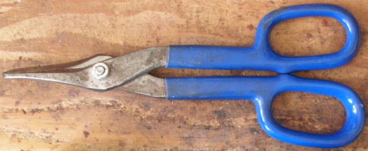
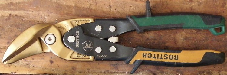
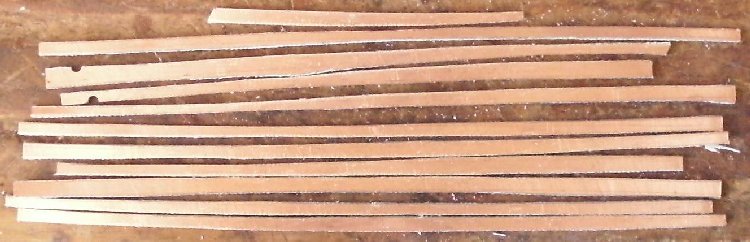
Cut approximately 32.5" of 1/8" strips from the PCB board you are using. This is used for all the traces of the transmitter. The original layout of the transmitter was modified to use 1/8" wide traces to simplify the Manhattan build of the transmitter. There are many kinds of tin snips but the one below is the best to use as it allows longer cuts through the PCB material without too much bending of the strips. Others that have an angle between the cutters and the handle require too much of a bend of the strips to be useful. |
|
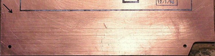
The strips will curl and twist when cutting with tin snips. Cut the strips with small cuts at a time working your way through the length of the PCB. After the pieces are cut, use two pliers going through the strips 2 to 4 times bending it a little at a time to keep them from breaking. Lay them down on the work bench to check them. The strips below are not perfect but good enough to work on the PCB. Only a few long ones will be needed. |
|
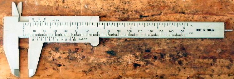
If you break them and don't get a couple of long pieces for the long runs, no problem, you can place them next to each other on the layout and then solder them together after Super Gluing them to the transmitter board. Second, measure the large and small blocks of the PCB pieces and cut them. A inexpensive plastic micrometer makes it easy to transfer the sizes of the blocks to the PCB for cutting. |
|
The PCB board with all the 1/8" traces Super Glued on the PCB. It is a little tricky to get them all glued and you can't help but get a little on the end of your fingers. Sometimes the Super Glue sticks hard very quickly so you have to be accurate when you lay the pieces down. A set of Tweezers can help a lot. |
|
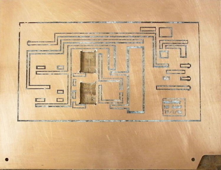
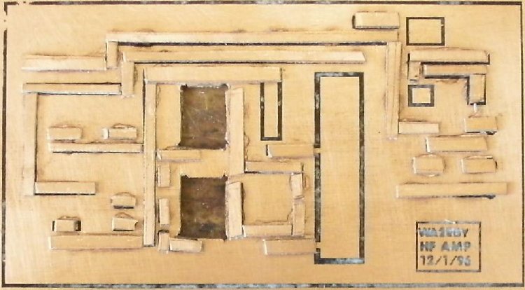
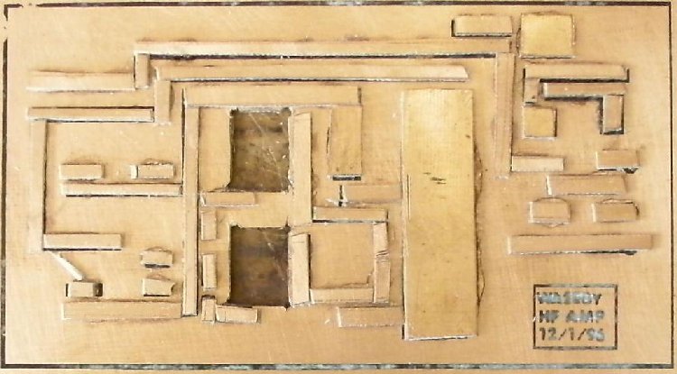
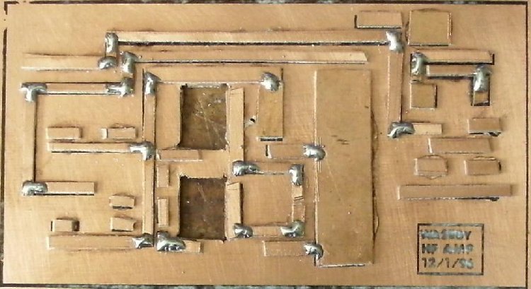
The board complete with all traces and rectangles. |
|
Fire up the soldering gun and solder the traces where they are broken, mainly at the corners, and solder what pads need to be soldered to traces. The following picture can be a guide to help you solder all the required places. On ones that are difficult to bridge, use a short piece of bare wire across the gap. It is a good idea to use a short piece of wire across all the bridges to make sure they stay connected when soldering on the parts, or double check the bridges after soldering on the parts. You will quickly find the ones that unsoldered when testing the completed transmitter. |
|
|
You are now ready to install the parts!Go to WA2EBY Manhattan Style Build. |
Send E-Mail || Amateur Radio Receivers || Back to Ham Radio Instructions for the Blue Lightning Transceiver