


|
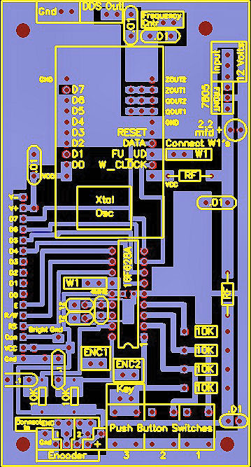
____1 - 9/64" Drill bit and drill Drill the four holes near each corner of the board, marked with an arrow, with the 9/64" drill bit. This is necessary so that the spacers/screws sent with the kit will fit through the PCB. 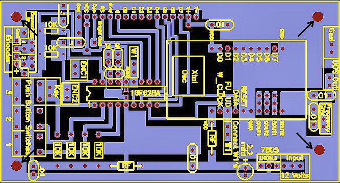
 ____1 - Narrow .01 capacitor, This cap has .02" pin spacing and goes in the exact middle (four pins on each side of the cap) of the PIC on the bottom side of the board to bypass the B+ to Gnd. It is placed in two holes between the two rows of pins for the PIC. Look carefully in the picture below to locate where it is soldered. After soldering, clip the leads on the top side of the board as close to the board as you can. 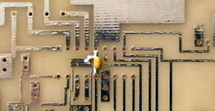  ____1 - 18 pin socket for the PIC. Notice the notch on one end of the socket and match it to the notch on the footprint on the PCB. Solder two pins to the PCB (diagonal opposite to each other), while holding the socket against the top side of the PCB. Then solder the other pins. Please Note: Getting the pins soldered correctly to this board means that the DDS has a 99% change of working on the first try. But mess up here and it may not work at all! Look at the pictures following to see what mistakes to look for. Use a magnifying glass to double check your soldering - PLEASE! 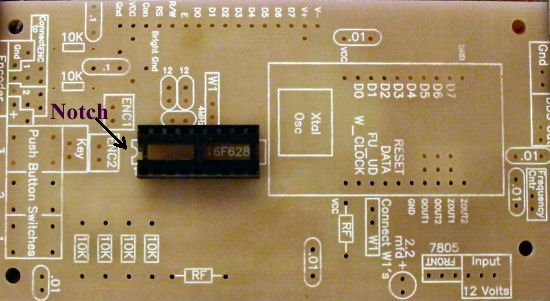 |
|
Look at the errors below pointed out by the arrows.
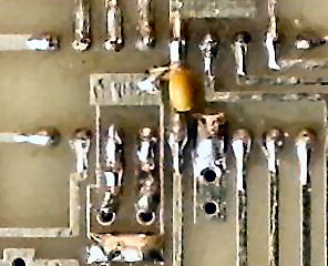
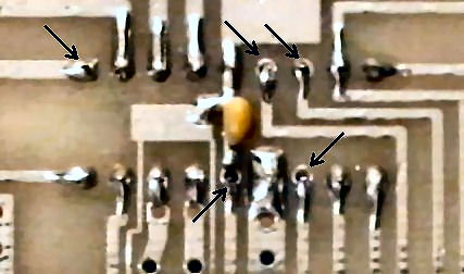 Your soldered pins should look like the ones below.
  ____4 - 10K resistors 1/4 Watt 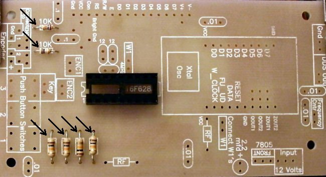  ____1 - Narrow .01 capacitor, This cap has .02" pin spacing 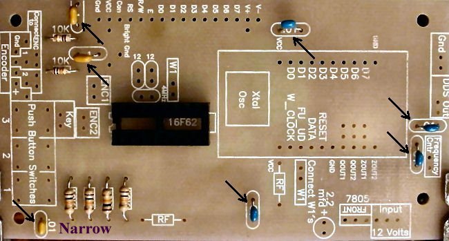  ____2 - 12pf capacitors, marked 12 with a black top 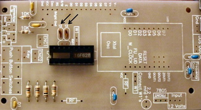  ____1 - 4.000MHz crystal, bend leads before inserting and soldering. Try to have it lay flat above the 12pf caps. 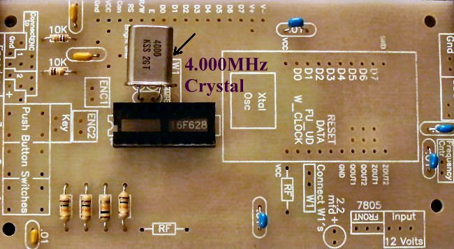  ____1 - 7805 Regulator 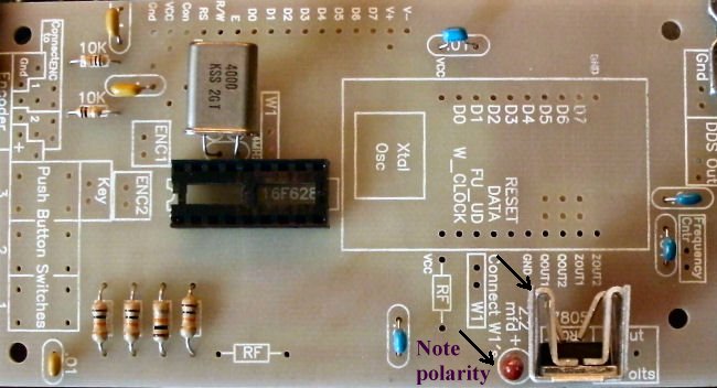  ____2 - RF Chokes Install the RF Chokes. 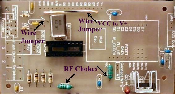  ____1- 16 Pin Female Header Install the Female Header and solder one pin. Make sure the header is straight, if not, reheat the pin and straighten. Finish soldering the pins. Check with a magnifying glass to make sure all solder joints are good. There are several ways to connect the display to the board. This one uses a 16 pin female header on the PCB. Two 16 pin male/male cables are soldered to the display. The other end of the double male cables are plugged into this female header. The outer 6 pins on both sides of the 16 pins are used. Two 6 pin Male/Male cables are supplied with the kit about 9" long. Colored wires help to connect the cables at both ends. Sorry, forgot to put pin numbers on the board. Note them on the board below. Use a black marker to write them on the board so you can see them when connecting the cables. 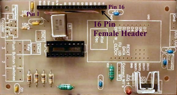  ____1 - LCD Display, 16 by 2, blue background with white letters. ____2 - 6 pin male cablesNOTE: Pin numbers - 1 and 16 - are clearly marked on the back of the display. Solder the two 6 Pin cables to the display on each end of the 16 Pin footprint. 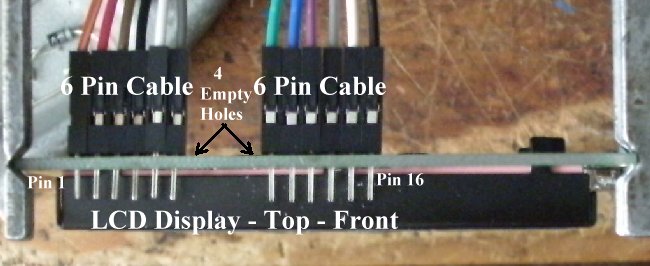   ____1 - 16F628A PIC Chip Follow the next two steps:1. Install the 16F628 PIC. The pins may be spread out slightly. Press them together so the PIC installs into the socket easily. Note the notch on one end of the chip and match to the notch on the footprint and on the 18 pin socket. 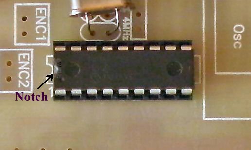 2. Hook up the display to the PCB (Pin 1 to Pin 1 and Pin 16 to Pin 16. Note the orientation of the boards. There will be four empty holes between the cables on both the DDS VFO PCB and the display.
Apply 12 Volts (with clips) to the 12V connection on the right side of the 7805 regulator (opposite the tantalum cap) and Ground connection to the ground plane on an edge of the board. The Display should light up and you should see what is shown in the picture below. 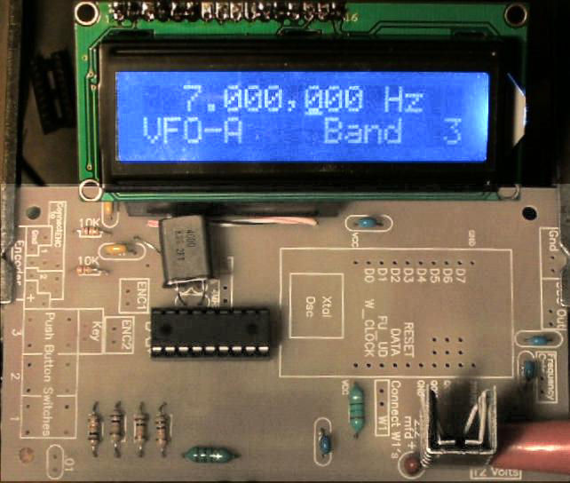  ____3 - PC mount Push Button Switches. 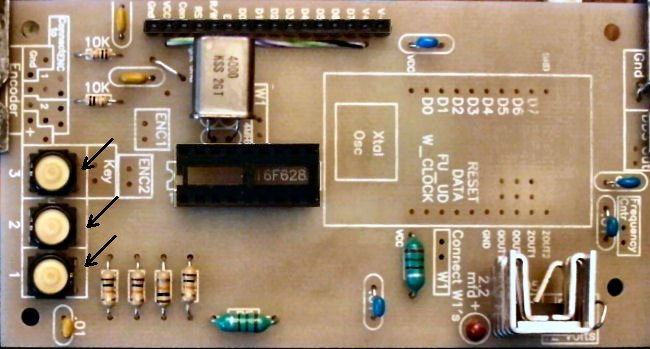 Special instructions: With the inner row of pins, solder the pins that connect to the traces and large pad. You don't need to solder the ones that don't connect to any traces. 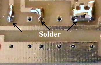 With the row of pins next to the edge of the board, solder the outside pins of Switch 1 and Switch 3 as shown below. 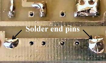 Cut the inside pins (Switch 1 and 3) flush with the bottom of the board. With Switch 2, cut one of the pins flush with the bottom of the board, then bend the other lead over flush with the board. 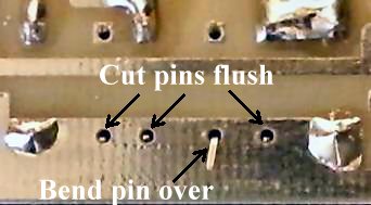 Solder with as little solder as you can to get a good ground connection. 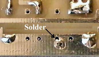  ____8 - Loops The ends of the jumper wires can be installed inside one of the holes at the locations if you don't want to make a bunch of loops. If you will be experimenting with different encoders, you may want to install loops at the encoder jumpers in case they need to be reversed. 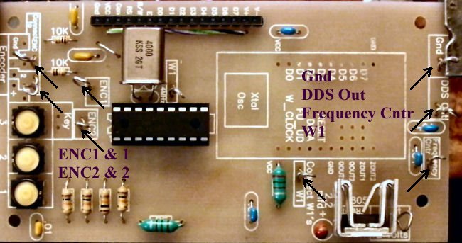 ____3 - Jumpers, 1 at 1-3/4" long, and 2 at 3/4" long 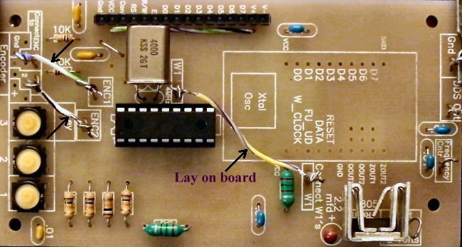  ____1 -China DDS Module. Notice location of the Xtal Oscillator and match to the footprint on the PCB. Also, outline of DDS footprint should match placement of the module. Push module through holes and solder. Jumper can go under the module, keep it in front of the module's pins as shown in picture. 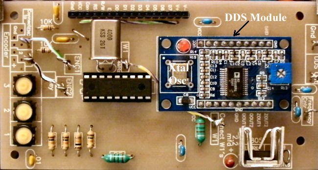  ____1 - Optical encoder First trim the leads at the end of the cable as shown below. About 3/16" long. Notice the black lead on one side - that is the ground.   Solder the leads onto the DDS VFO board. Notice the Ground and + leads are on opposite sides of the cable. Solder them to the board as shown below using the rows of holes next to edge of the board. Note: Best to tin the leads before inserting into the PCB holes. The stranded leads of the Encoder are very thin and if they hit the edge of the hole, they will bend, making it difficult to insert. Trying to twist the strands together can be difficult. Right after trimming the insulation off a lead, tin immediately. 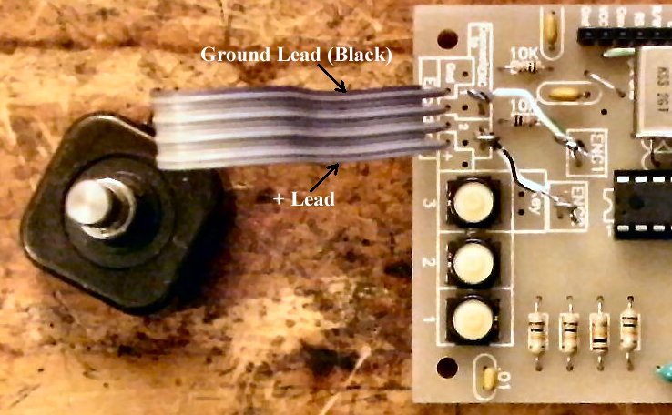  |
 Pushbutton OperationPB1If depressed during power-on, enter Calibration mode. The display shows 10,000,000 CAL and 10 MHz signal is generated. The output should be monitored with a Frequency Counter, or other means, for correct frequency. While holding PB1, the encoder is used to adjust output frequency to 10 MHz. Once output frequency is correct, release PB1 and turn encoder. Normal operation then starts. It is not necessary to hold PB1 if the encoder is not moved allowing entering calibrate mode and waiting for thermal stabalization before calibrating. Momentary depression moves cursor to the left one decade position. The cursor will wrap from highest decade to 1 Hz decade. Holding down for one second will start automatic movement of cursor to left every 1/8 second. When held down for 2 seconds, along with PB2, store the current frequency at the current band number in EEPROM. The display will show 'UpdatedXX" where XX is the current band number. Pushbuttons are then released. The frequency stored will be the start frequency when this band is selected. Used with PB2 to change startup band in EEPROM. PB2Momentary depression moves cursor to the right one decade position. The cursor will wrap from the 1 Hz decade to the highest decade. Holding down for one second will start automatic movement of cursor to right every 1/8 second. Depressing PB2 and moving encoder before one second will enter band change mode. Moving the encoder will cycle through all the bands configured and releasing PB2 will select last band displayed. While in band change mode, PB2 still depressed, PB1 is pressed and both are held for 2 seconds, the current band number is written to EEPROM as the power-up band. Display wil show "Updated" for one second and then "Initband" for one second. Both pushbuttons are then released. PB3PB3 is used for the transmit function. When grounded, it removes the offset and outputs the correct frequency used for transmitting. The change is frequency is very fast as well as changing back to receive frequency with the offset. The "KEY" notation on the board is where a key, either hand key or an iambic keyer, is connected to send CW. This KEY is also wired to the relay coil, which is grounded to activate, to send the signal to the transmitter. A diode, the anode connected to the KEY is used to isolate it from the keying line. Also, a diode (anode side) is connected to the "KEY" connection of the relay. Then both cathodes are connected together for the connection to the keyer, which grounds the two cathode diode connections when keyed. |


Send E-Mail || Amateur Radio Receivers || Back to Instructions for the SuperLuminescent Receiver

