|
Different sizes of spacers and screws will be sent with the kit. Spacers that fit 4-40 screws will not need any modifications. Spacers that fit 6-32 screws will need the following modifications:
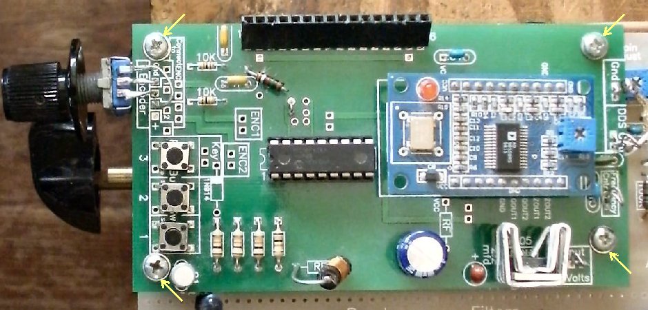
Note: If you are mounting this board on an ELR with the spacers/screws sent with the kit, drill the holes at the corners as shown below. ____1 - 9/64" Drill bit and drill Drill the four holes near each corner of the board, marked with an arrow, with the 9/64" drill bit. |
|
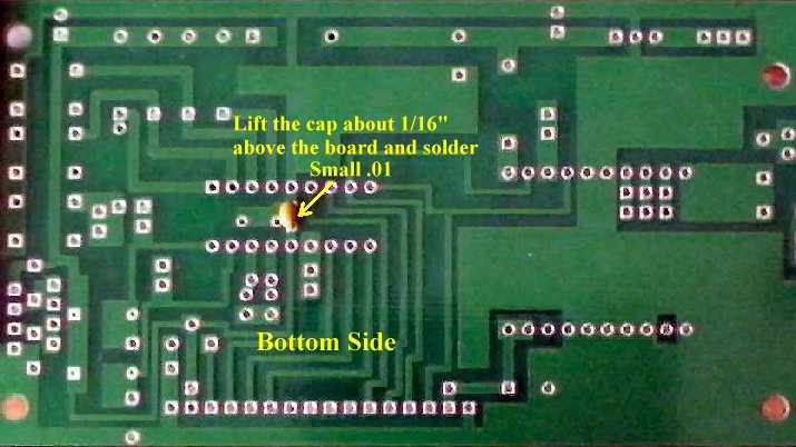
____1 - Narrow .01 capacitor, This cap has .02" pin spacing and goes in the exact middle (four pins on each side of the cap) of the PIC on the bottom side of the board to bypass the B+ to Gnd. It is placed in two holes between the two rows of pins for the PIC. Look carefully in the picture below to locate where it is placed. Lift the capacitor about 1/6" above the board and solder. Bending the leads on the opposite side of the board can hold it in place while soldering. |
|
After soldering, clip the leads as close to the board as you can. |
|
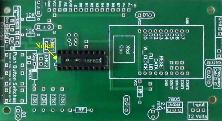
____1 - 18 pin socket for the PIC. Notice the notch on one end of the socket and match it to the notch on the footprint on the PCB. Note! Make sure the socket fits flat against the board. If not, clip the capacitor leads closer to the board. Solder two pins to the PCB (diagonal opposite to each other), while holding the socket against the top side of the PCB. Then solder the other pins. |
|
Use a magnifying glass to double check your soldering on the socket pins. 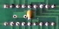 |
|
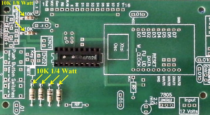
____4 - 10K resistors 1/4 Watt, Bend leads slightly away from the body of the resistor for easy insertion. |
|
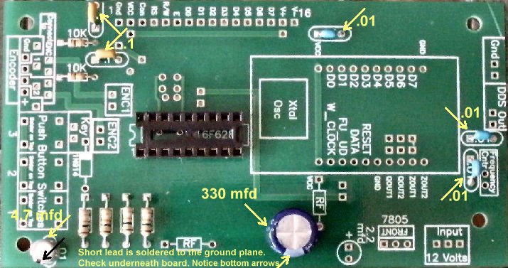
____1 - 4.7 mfd Electrolytic capacitor, put in the place of the narrow .01 footprint. Short lead, negative pin, is soldered to the ground plane, see picture below. |
|
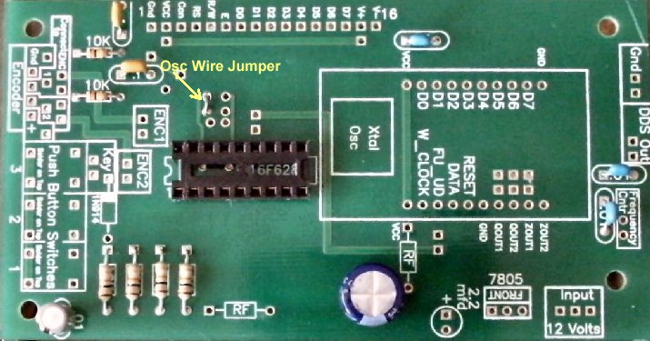
____1 - 1 inch wire jumper, a cut resistor lead will work This wire sets the Oscillator for the PIC. This oscillator type is 'Internal Oscillator and the frequency is set by a resistor from Pin 3 to ground. In this case the resistor value is zero, which sets a Frequency of 10.4MHz for the Internal Oscillator. This allows the use of either an optical (128 step) or mechanical encoder (24 step). The Configuration Word for this Oscillator is ER_OSC_NOCLKOUT. Notice the other solder points around this area, Pin 3 and Pin 4 of the PIC. This allows putting in a Crystal Osc function if desired. The internal oscillator was used because it radiated the lowest RF signal from the PIC, making it quieter to use with the receiver. |
|
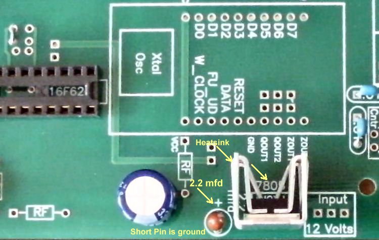
____1 - 7805 Regulator, Front of part is oriented toward center of board. |
|
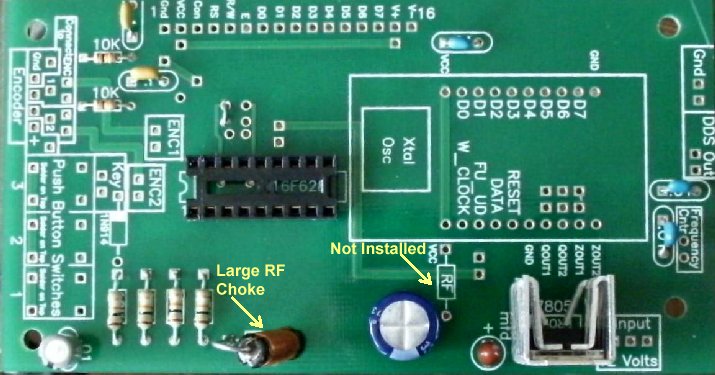
____1 - Large RF Choke, mounted vertically |
|
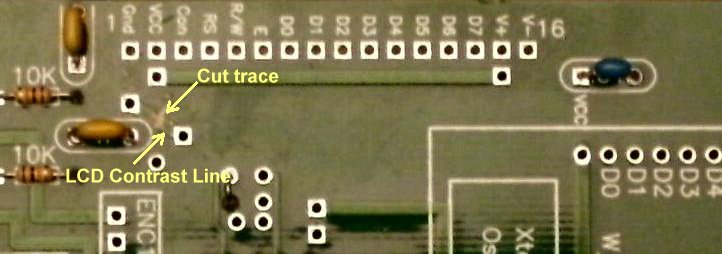
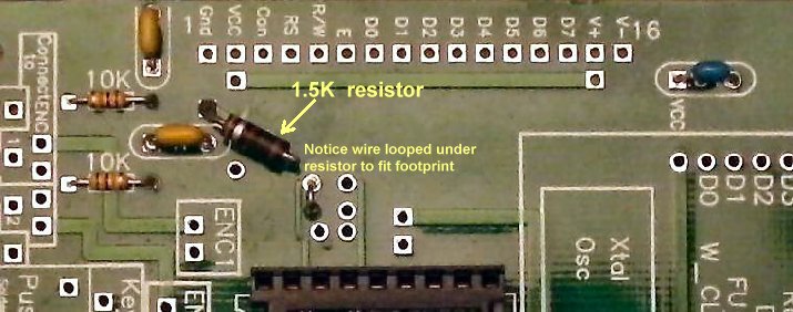
The following may have already been done. Check to make sure the trace is cut with a multimeter to see that there is no connectivity between the holes. Notice in the following picture where a trace is cut. This trace controls the brightness of the LCD. Some of the LCDs shipped with the kit are too bright and you can't see the lettering with these two holes shorted. When the bright control on the LCD is grounded it runs full brightness. It was found that a 1.5K (a 1K, 1.2K or 1.5K) resistor provides the right brightness for all the LCDs shipped with the kit so this trace needs to be cut and the resistor soldered in the holes on each end. Use a utility knife and cut through the trace at an angle and then cut again at an opposite angle or straight down to cut the trace. Check with a multimeter to make sure the trace is cut. |
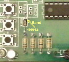
____1 - 1N914 Diode, match Black band of Diode to the white band on the footprint
 |
|
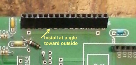
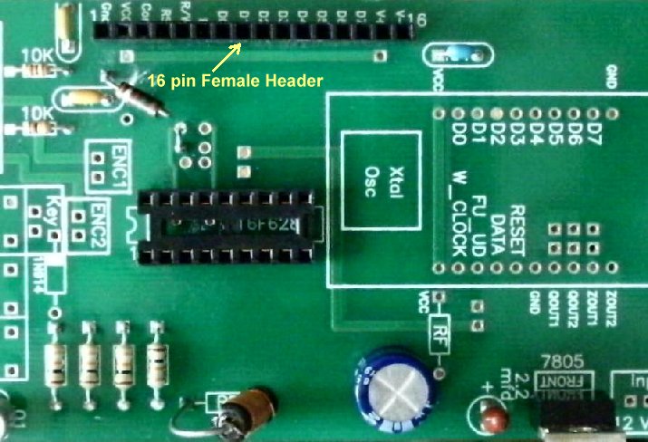
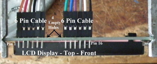
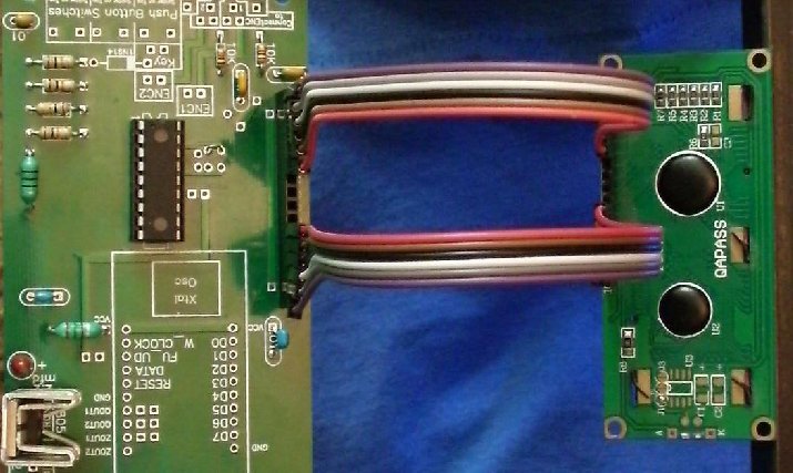
Check with a magnifying glass to make sure all solder joints are good. There are several ways to connect the display to the board. This one uses a 16 pin female header on the PCB. Two 6 pin male/male cables are soldered to the display. The other end of the double male cables are plugged into this female header. The outer 6 pins on both sides of the 16 pins are used. Two 6 pin Male/Male cables are supplied with the kit are about 9" long. Colored wires help to connect the cables correctly (Pin 1 and Pin 16) at both ends. |
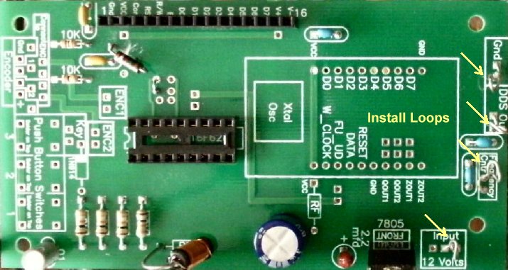
| ____3 - Loops, 1 1/4" inch bare wire bent into a loop. See Construction - Making Loops |
|
____1 - LCD Display, 16 by 2, blue background with white letters. ____2 - 6 pin male cablesNOTE: Pin numbers - 1 and 16 - are clearly marked on the back of the display. Solder or connect the two 6 Pin cables to the display on each end of the 16 Pin footprint. Make sure there are no crossed wires! They should all be in a row. If you find a crossed wire after soldering, since they are individual connectors, you can remove the ones crossed easily and correct the error. |
|
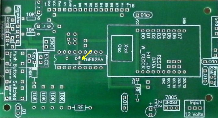
____1 - 16F628A PIC Chip Follow the next two steps:1. Install the 16F628 PIC. The pins may be spread out slightly. Press them together so the PIC installs into the socket easily. Note the notch on one end of the chip and match to the notch on the footprint and on the 18 pin socket. 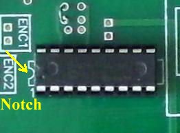 2. Hook up the display to the PCB (Pin 1 to Pin 1 and Pin 16 to Pin 16. Note the orientation of the boards. There will be four empty holes between the cables on both the DDS VFO PCB and the display. |
|
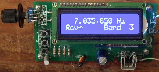
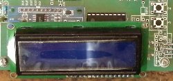
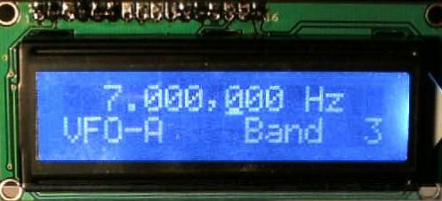
Apply 12 Volts (with clips) to the 12V connection on the right side of the 7805 regulator (opposite the tantalum cap) and Ground connection to the ground plane on an edge of the board. The Display should light up and you should see what is shown in the picture below. |
|
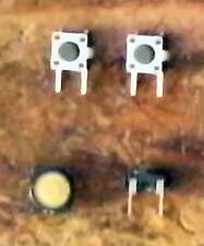
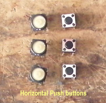
____3 - PC mount Push Button Switches. |
|
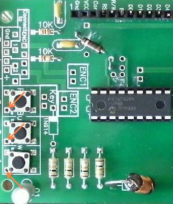
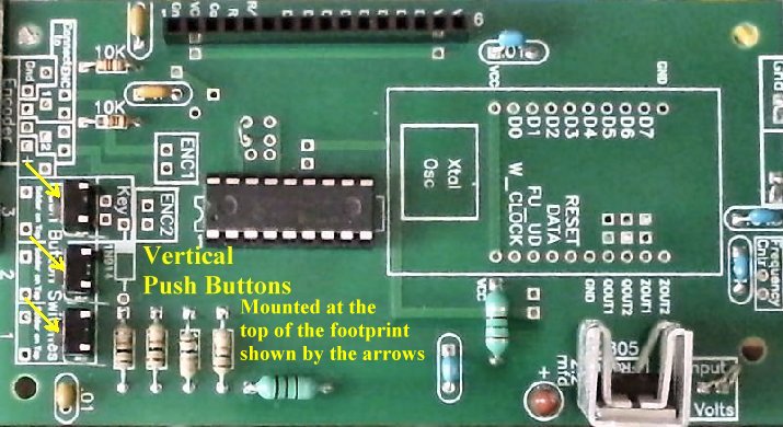
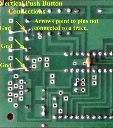
There are three kinds of Push Buttons, one vertical and two horizontal. The vertical ones have two leads (Upper left hand picture) and the horizontal have four. The horizontal ones have two leads connected to one side of the switch and two leads connected to the other side of the switch. The vertical buttons need a jumper to ground one side of the switch. The picture below shows the vertical ones, both top and bottom. The jumpers needed are shown in the following picture. Notice that the pins not connected to a trace are jumpered to ground (Holes on the left side as shown in the picture). |
|
The black horizontal ones (with large white buttons) are soldered onto the board with no modifications. They drop into the holes for the switches. The silver ones with the small buttons need one pin cut off before soldered onto the board. Notice the red arrows in the picture below and the pin that needs to be cut before mounting onto the board. They may already be cut before shipping.
Be careful pushing them into the board to get them to set flat on the board. |
|
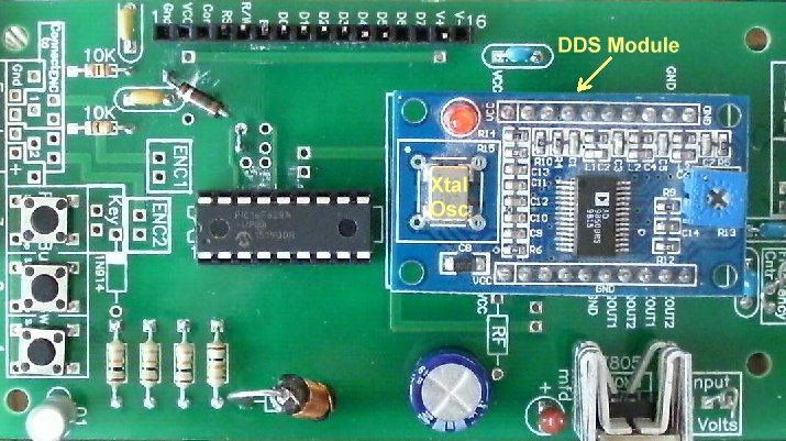
____1 -China DDS Module. Notice location of the Xtal Oscillator and match it to the footprint on the PCB. Also, the outline of DDS footprint should match placement of the module. Push the module through the holes and solder. |
|
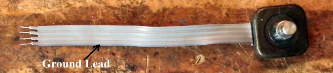
____1 - Optical encoder First, trim and tim the leads at the end of the cable as shown below about 3/16" long. Notice the black lead on one side - that is the ground. Note: Best to tin the leads before inserting into the PCB holes. The stranded leads of the Encoder are very thin and if they hit the edge of the hole, they will bend, making it difficult to insert. Trying to twist the strands together can be difficult. Right after trimming the insulation off a lead, tin immediately. |
|
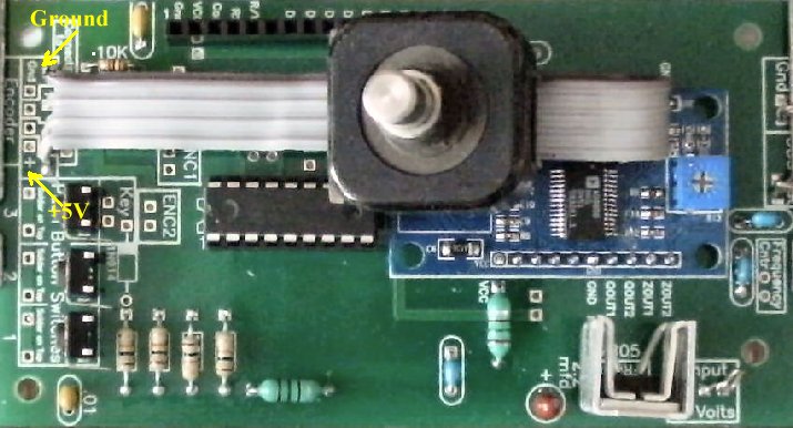
Solder the leads onto the DDS VFO board. Notice the Ground and + leads are on opposite sides of the cable. Solder them to the board as shown below. You may find that holding the encoder against the top of the board (the board being upside down) will keep the leads in the holes while soldering on the bottom side. Solder the Gnd and +, first, then the cable will be held to the board while soldering the center leads. Be careful handling the Optical Encoder leads, as they break easily with too much movement. |
|
____1 - Mechanical Encoder It is easier to use a mechanical encoder if you are going to use it on top of ELR Board 1 above the VFO. The pins for connecting the mechanical encoder with a center pin ground are not correct on the board. The left pin of the encoder is straightened out and the ground (center pin) is inserted in the Ground plated through hole as shown below. 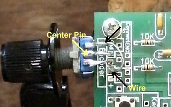 Clean the green solder mask from underside the board where the tabs on each side of the mechanical encoder touch the bottom of the PCB. The tabs will be soldered here to provide stability for the encoder. 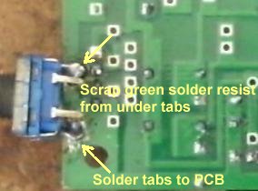 ____Solder the center pin (Ground) and right hand pin (to the hole in the box labeled number 1) of the encoder to the board while holding the tabs against the underside of the PCB. 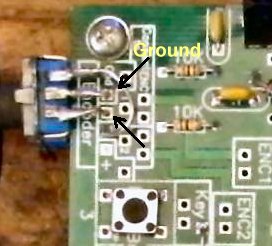 ____Solder the tabs to the ground plane underneath the board. 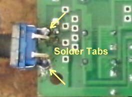 ____Then a wire is soldered to the straightened pin and connected to the hole in the box marked number 2. |
|
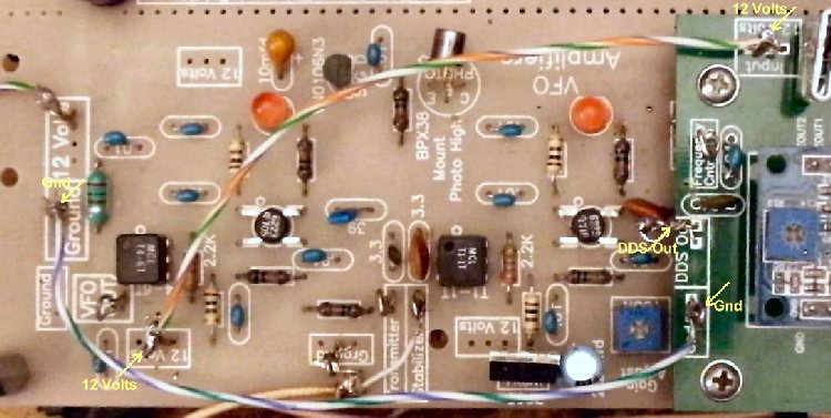
On the ELR boards marked 10/1/2000 and 10/1/2005, three holes will match the board. The one on the top right (in the above picture) will not match a hole and the DDS will be mounted with the other three holes. The ELR boards marked REV 3 3/4/2015 all four holes will match. Attaching DDS Out to the First VFO MOSFET AmplifierLift the lead of the 3.3 capacitor as shown below and attach to the DDS VFO Out of the DDS VFO board. They should be very close in proximity. You might be able to get the lead into the DDS VFO Out connection by threading the lead into the hole when mounting the DDS VFO board above the ELR VFO. 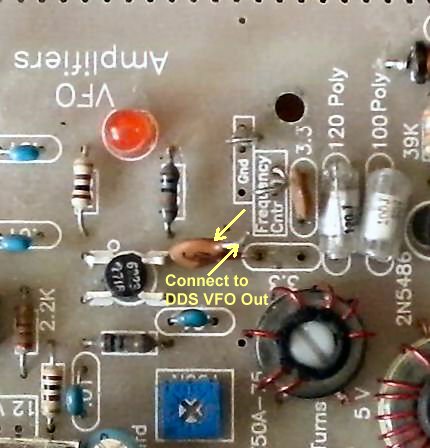 Disconnect the 5 Volt power to the VFO on the ELR board. You can remove the 5 volt regulator or one of the leads of the RF Choke at the back of the VFO labeled FT50A-75. The lead from the coil right next to this text (FT50A-75) will remove 5 volts to the VFO and be easy to remove. 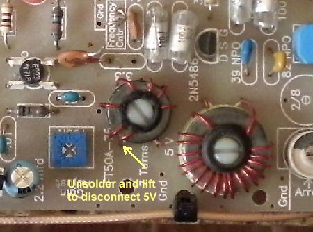 Attach 12 Volts to the 12 Volt box on the edge of Section 1 (or at the back) and attach a Ground from the DDS VFO to the Ground at the back of the Section. Connect DDS Out to the 3.3pf Capacitor. |
DDS VFO InstructionsPushbutton OperationStarting at the rotary encoder, the switches are labeled 3, 2, and 1. Number 1 is at the front right edge of the DDS VFO board. Operation when Listening or QSOingWhen the receiver is first turned on, 40 Meters will be the displayed band. After the first turn on, the last band/frequency will be saved and loaded on start up. To change bands, hold down/push Button 2 (middle button) and turn the encoder (within one second) to the band you want. You will be at the start of the band - XX.000 The default digit will be the .01 digit, and tuning will be fairly slow through the band. If you want to scan the band quickly to find signals, push button 1 (right hand button) and it will move to the .1 digit for quick tuning through the band. When you find a signal you wish to tune in, push button 2 (middle button) to move the cursor to the .01 digit and you can tune in the signal precisely. If you wish to transmit on this frequency, push button 1 (right hand button), and tap your key. You will see that the Band number will now be displayed on the bottom line of the display and will show your Transmit frequency. Your transmit frequency will remain the same until you hit Button 1 and hit your key at a different frequency. Once your transmit frequency is set, you have RIT and can move your receive frequency anywhere you like - transmit frequency will remain the same. When you set your Transmit frequency, Rcvr will remain on the display. When you transmit, Xmtr will show on the display with the transmit frequency, even when returning to receive, until the encoder is moved to a different receive frequency. The receive frequency will remain the same even though the transmit frequency will be shown during the QSO, unless you RIT and the new receive frequency will be shown until you transmit again. If you finish your CQ or QSO and move to a different frequency and transmit without setting the new frequency first, your old transmit frequency will show on the display. Push Button 1, and tap your key to set the new transmit frequency. PB3Used with PB1 to set Transmit FrequencyPB3 is used for the transmit function. When grounded (Keyed with key or keyer), it removes the offset and outputs the correct frequency used for transmitting. The change to transmit frequency and changing back to the receive frequency with the offset is very fast. Up to 40 wpm has been no problem. When you transmit, the Transmit Frequency and Xmtr will remain on the display. The receive frequency will stay the same. If you move the Rotary Encoder, the Receive Frequency and Rcvr will be displayed. Pressing PB1 and taping the key/keyer (connected to PB3) at the same time sets the transmit frequency. After setting the transmit frequency, you are free to turn the Rotary Encoder to any receive frequency you desire. For working DX up1, you move the frequency up one 1kHz, set the transmit frequency and then move back to the DX station frequency. See PB3 for more information. PB2Cursor to RightMomentary depression moves cursor to the right one decade position. The cursor will wrap from the 1 Hz decade to the highest decade. Holding down for one second will start automatic movement of cursor to right every 1/8 second. Band ChangeDepressing PB2 and moving encoder before one second will enter band change mode. Moving the encoder will cycle through all the bands configured and releasing PB2 will select last band displayed. PB1Cursor to LeftMomentary depression moves cursor to the left one decade position. The cursor will wrap from highest decade to 1 Hz decade. Holding down for one second will start automatic movement of cursor to left every 1/8 second. Set Transmit FrequencyPB3 is connected to your key/keyer. You press PB1 and hit the key, the transmit frequency is set to the frequency on the display. PB1 can be connected to the switch on a mechanical encoder for quick setting of the transmit frequency (other terminal of switch is connected to ground). The transmit frequency will not be transmitted or displayed when you set it. If you want to check the transmit frequency, send one dot (will be transmitted) and Xmtr with the transmit frequency will be displayed. You can move the receive frequency as desired (for RIT function); the transmit frequency will remain the same. If you finish your QSO and move to another one at a different frequency, remember to reset your transmit frequency. Press PB1 and hit the Key to set the new frequency. If you forget and see that you are transmitting at the old frequency, press PB1 and hit the key to set the correct transmit frequency. Key ConnectionThe "KEY" notation on the board is where a key, either hand key or an iambic keyer, is connected to send CW. This "KEY" connection is grounded to activate the transmit function, activate the T/R switch, and send the signal to the transmitter. A diode, the anode connected to the output of the PIC to PB3 is used to isolate it from the keying line. Also, a diode (anode side) is connected to the PNP switch of a T/R switch. Then both cathodes are connected together for the connection to the key/keyer, which grounds the two cathode diode connections when keyed. There are two KEY connections, one on the DDS VFO at PB1, and a second one at the T/R switch labeled "DDS VFO Key" at the edge of the board. This second connection is the easiest to connect the line to the keyer. Tuning Range of the DDS VFOThe bands are chosen with the DDS VFO by pushing Button 3 and turning the DDS VFO knob within one second. The DDS VFO will scroll through the bands until it reaches the one you want and quit turning the knob. The bands on the DDS VFO are 160/80/60/40/30/20/17/15/10. The next band is 200kHz, which does not have the offset programmed and is a signal generator that outputs the exact frequency it is showing. It is used to determine the center frequency of the crystal filters so it can be programmed into the offset frequency if the crystal filter frequency is changed. To use this function, tune the 200kHz band near the frequency of the Crystal Filter frequency and peak the output at the S-Meter. Use the 100 Hz or 10 Hz tuning digit to find the peak. The peak frequency is then the offset frequency put into the programming for the bands. The next band shows 0 and is a general coverage band that has the offset programmed (plus 3.546 MHz) and can be used to go to any frequency between the limits of the Bandpass Filters, below 60 to 10 Meters. The Band numbers showing on the display go from 1 to 9, 1.800 to 24.890 (160 to 12 Meters). On 10 Meters it shows :, on General Coverage band 0, it shows ;, and on 200 kHz, it shows >. I guess the original programming didn't go above a one digit number. This will probably be fixed in a future release, but it doesn't effect operation. Calibrate ModeCALIBRATE MODE is entered if PB_1 is pressed during power-on. The display is set to 10 MHz and remains fixed, even as adjustments are being made. If pushbutton is held pressed, then turning the shaft encoder will increase or decrease the value "osc" used to calculate the DDS control word. The basic calibrate adjustment rate is very low (on the order of a few cycles per turn of the encoder). A somewhat faster adjustment speed is available by pressing the encoder shaft or PB 3 down while turning. An external frequency counter on the DDS output is required to observe this adjustment. Alternatively, tune a receiver to the 10 MHz WWV broadcast and zero-beat the carrier. To exit calibrate mode, release the pushbutton and turn the shaft encoder one more time. The calibrated value of "osc" will then be stored in EEPROM memory. |
Send E-Mail || Amateur Radio Receivers ||
Back to the Blue Lightning Transceiver