PIC DDS VFO
|
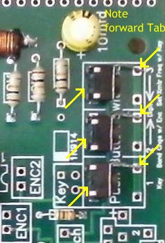
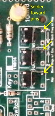
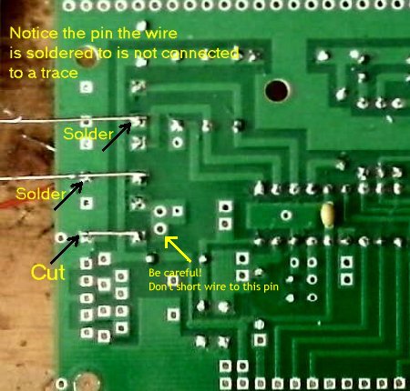
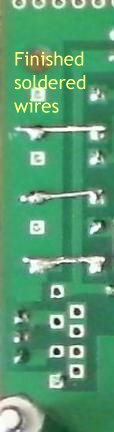
There are three steps to solder the switches on the bottom side of the board: The steps are shown below:1. Solder a wire to the switch - the connection that a trace does not connect to. 2. Solder the other end to a ground via as shown. 3. Trim excess wire. Do this to all three switches - only one step per switch is shown below, finish all steps on each switch. |
|
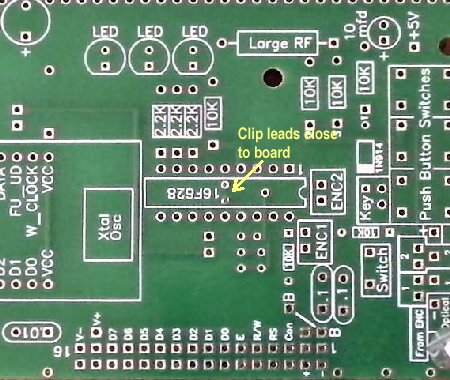
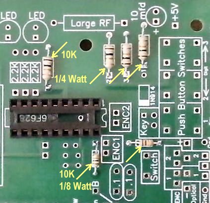
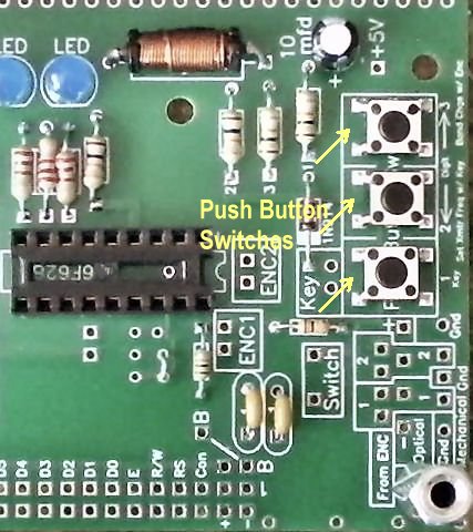
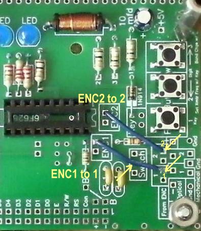
The Top Mounted Encoder requires moving the corner spacer to give room for a knob but is the most secure. Easy to use the encoder switch as you push down with stable operation. Top Forward Mounting Encoder is the most convenient to use. Four wires, two for the switch and two to ground hold the encoder firmly for easy rotation. The Bottom Forward Mounted Encoder allows the easiest access to the switches. Number 1 is rarely used so this isn't very important to do as switches 2 and 3 can be reached with the top mounting also. Review the instructions for each mounting first and decide which one you would like. Notice a small notch was made on the top corner (two pins) of the encoder to remove a curved spring to eliminate the clicking for effortless turning. Rotary Encoder Top MountingWhen using a Top Mounted Encoder, in order to use a knob the spacer at the corner will have to be moved to the right and the holes drilled with a 9/64" drill bit. The bottom spacer can be held with a nut and 2 screws will be needed at the new location for the upper spacer. The longer spacer 1 7/8" (double female) will be used between the boards and the smaller ones for the bottom. Note: The Mechanical rotary encoder included with the kit has a metal bottom. This will short out the pads underneath the encoder. Place a piece of black tape over the pads that will be under the encoder or place a piece of black tape on the back of the encoder as shown below. 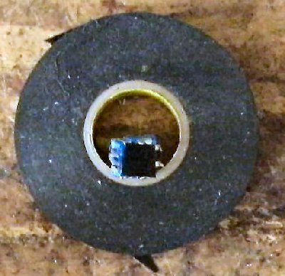 Connections need to be soldered between ENC1 to 1 and ENC2 to 2 in the encoder connection box. 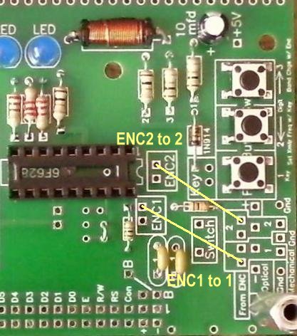 The connections to the box have to be soldered to the bottom of the board to prevent a short to the bottom of the encoder. Two lengths of 1" wire will be used. See pictures below. 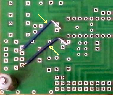 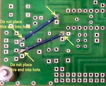 Install the encoder as shown below. There is a box labeled Switch through which the two leads will fit. This switch is connected to Button 3, which is used to set the transmit frequency with Button 1, connected to the transmit key (or pressing the key when connected). 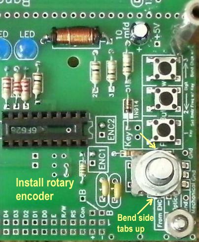 Note new location of the spacers in the above picture.
|
|
Bottom Mounted Encoder
When the encoder is mounted underneath the board, the rotation for increased frequency is reversed. The Encoder wires from the PIC have to be reversed so that turning the encoder clockwise will still increase the frequency. Use two 1-1/4" wires, one will go from ENC1 to 2 inside the encoder mounting box, and one will go from ENC2 to 1 inside the incoder mounting box. 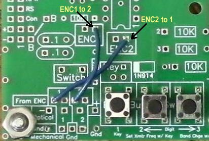 |
|
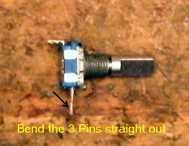
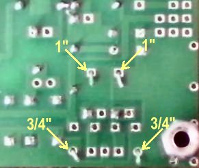
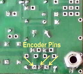
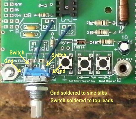
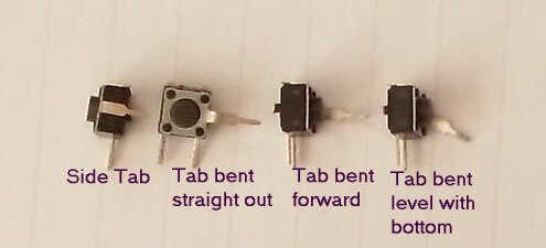
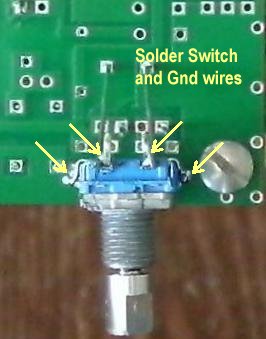
Two 1" bare wires (#22 or larger) are soldered in the Switch Box and two 3/4" are soldered in the two Gnd holes one each side of the mounting holes for the encoder. Make a small 90 degree bend at the top of the wires to hold them while soldering. 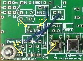 Next, install the encoder from the bottom side of the board and solder the leads at the top of the board. 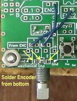 Turn the board over and solder the switch wires to the top two leads of the encoder. Straighten these wires and solder the leads close to the encoder as shown. Bend the side tabs forward and inward toward the body of the encoder. Solder the Gnd wires to the tabs on each side of the encoder and then trim extra lead length. |
|
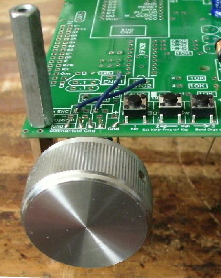
With this mounting, the longer 1 7/8" spacer is used on the bottom and the shorter spacer 1 1/4" is used between the boards. The switches are easily reached with this mounting. |
|
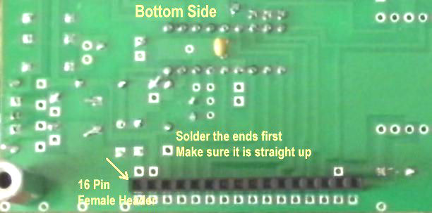
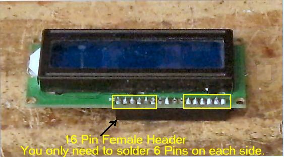
____1 - LCD Display, White characters with Blue Background ____1 - 16 Pin Female Header |
|
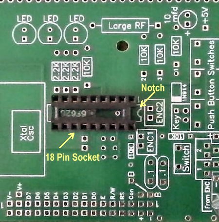
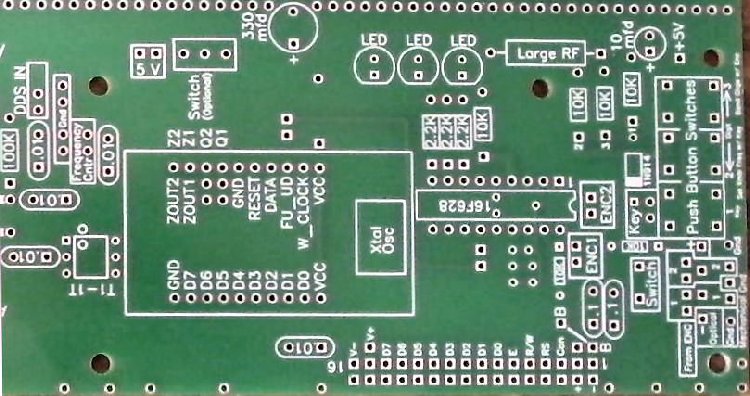
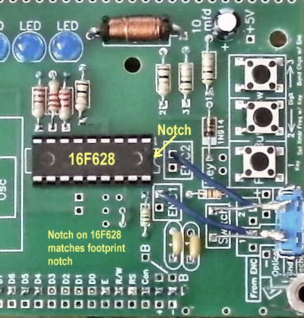
____1 - PIC IC 16F628 - Install on board, match notch on chip to notch on footprint
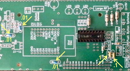
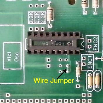
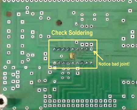
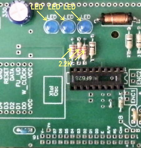
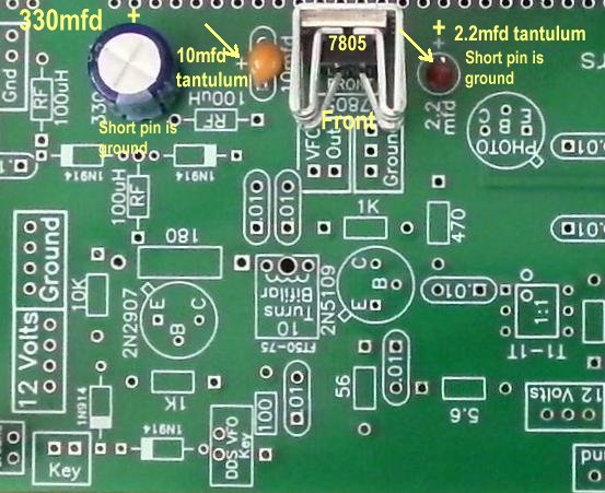
 ____1 - 1.5K resistor. The leads are bent underneath the resistor a little bit so it can go into the holes. There wasn't enough room for a regular resistor footprint. 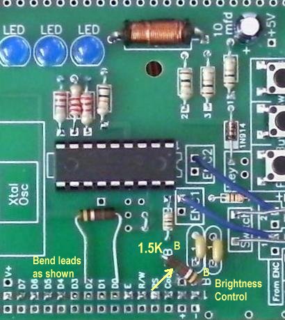 The white line between two plated through holes marked "B" determines the brightness of the LCD. A wire short between the "B" connections is full brightness. A 1.5K resistor has worked well for the LCDs purchased for the kit, but can be changed to any value for the brightness one desires. Soldering the resistor to the top of the plated hole makes it easier to change out. Power can be applied to the "12 Volts and Ground" box and the first test can be done. The LCD readout will be connected and 12 Volts and Ground from a 12 volt supply will be attached to the Loops just soldered onto the PCB. 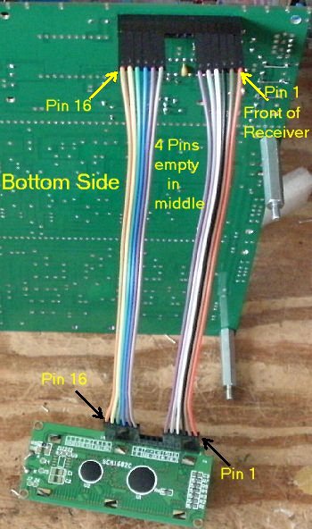 Attach 12V and Ground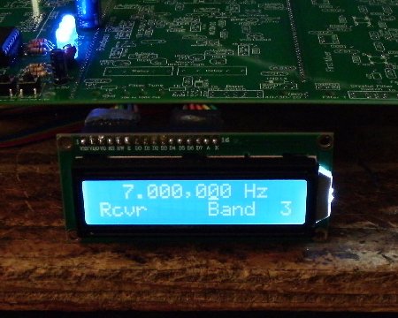 The display should read 7.000.000 at first power up. If the chip was tested it might show a different frequency. Switches 2 and 3 will move the cursor (2 left, 3 right). Switch 1 is used for Transmit Key function and will not do anything when pushed by itself. Pushing the encoder switch will move the cursor to the left. Push the encoder to engage switch (connected to Switch 2) and push Switch 1, Release the encoder, then push Switch 1 again. (Switch 1 is connected to the "Key" output.) You will see Xmtr on the display. Turn the encoder and you will see Rcvr and the frequency changing. To change bands, push Switch 3 and turn the encoder within one second. To change to a new Transmit frequency shown on the display, push the Encoder switch and press Switch 1, then press Switch 1 again to see the Transmit frequency. With a key connected to the Key Box, The Encoder switch is pressed with the the key tapped for either a dash or a dah for the new transmit frequency to be set. Tapping the key again will show the new transmit frequency. After testing, you can disconnect the cable from Board 1 and set the LCD aside. You will be mounting it with plastic ties right under Board 1 when you get to Mounting/Testing Board 1 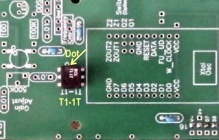 ____1 - AD9851/AD9850 DDS Module, Inside the DDS footprint, on the side toward the PIC, you will see a small square labeled "XTAL OSC", make sure you insert the AD9850/1 DDS Module with the silver square (the crystal oscillator) on the board above the "XTAL OSC" on the footprint.  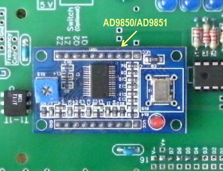 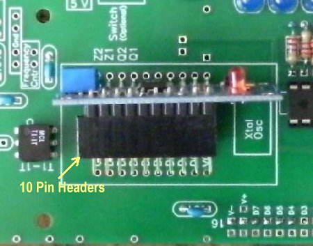 If desired: Two 10 pin plug in spacers can be soldered onto the PCB board for the AD9850/AD9851 for easy changing in case of failure or change of module. Some of the modules do not have the exact pin spacing across the board and the spacers are needed to install the module. You can check this by trying to install the module. If it does not quite fit, then you have to use the spacers. Have the plug in spacers installed on the DDS module when soldering to make sure the DDS fits into the spacers easily after soldering onto the board. Double check soldering with a magnifying glass, sometimes the header pins have trouble taking solder. |
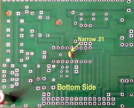
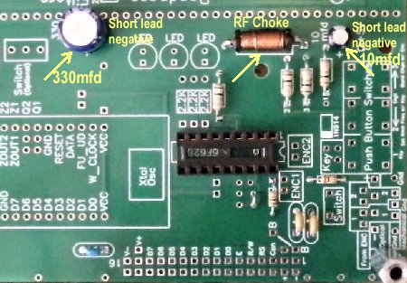
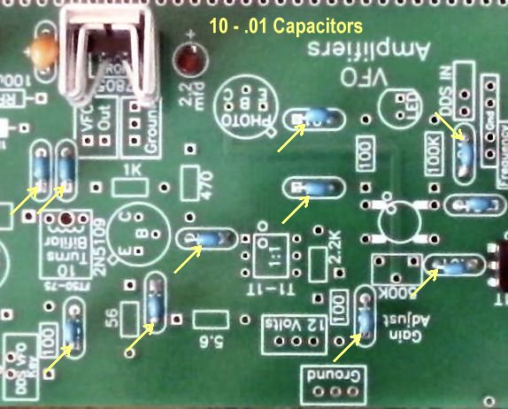
DDS VFO Amplifiers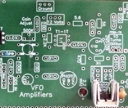 The parts for this section are in Bags 1 through 6 as noted with the parts.____10 - .01 capacitors (Bag 3) |
|
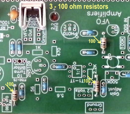
____3 - 100 ohm resistors (Bag 3), (brown, black, brown) |
|
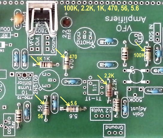
____1 - 100K resistors (Bag 3), (brown, black, yellow) |
|
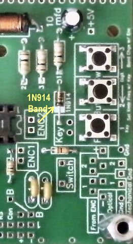
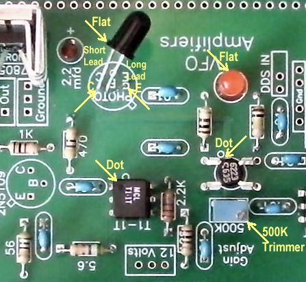
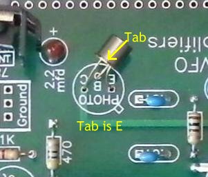
____1 - MOSFET (Bag 2), (Picture) static sensitive part, touch a ground wire before taking it out of the bag, notice the dot on MOSFET (may be difficult to see, hold at an angle to a light source and you can see the shadow of the dot), the dot is located to the left of the second line of the text on the MOSFET. A dot is placed outside the footprint so that you can double check your placement after it has been inserted or soldered to the PCB. The leads on each side of the part need to spread apart slightly to fit the footprint. See Picture of MOSFET for details. With the black colored Phototransistor the short lead (has a flat on the side) goes into the "C" connection. The long lead (round side) goes into the "E" Connection. Mount phototransistor as high as possible using all the lead length. Push the part through the holes, then spread the leads slightly, then pull back up. This will hold the part while soldering. With the BPX 38, Note the picture below in mounting the part. The Tab is the E connection, B is between the two leads, and C is opposite E. The Phototransistor can be bent (90 degree angle) towards the First Mixer in Section 3 of the board as shown in the pictures. ____1 - T1-1T Minicircuits transformer (Bag 4), Note the dot on the T1-1T transformer and match the dot on the silkscreen. The dot on the outside of the footprint can be seen after the part is mounted so that you can double check proper mounting. |
|
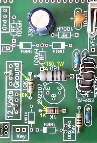
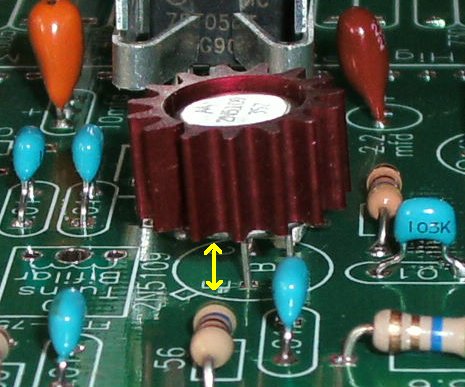
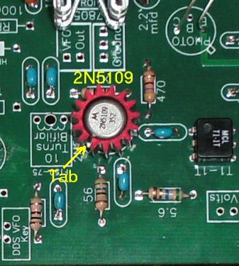
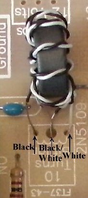
____1 - 2N5109 transistor and heatsink (Bag 5) Push the Heatsink on the 2N5109 first. There will be other types of heatsinks in the kits, so make sure you know where the tab is before mounting onto the board.
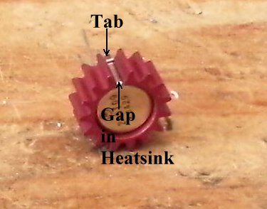 Solder 2N5109 with Heatsink about 3/16" to 1/4" above PCB. Note location of tab. Solder one pin, straighten up the transistor, then solder the other two leads. |
|
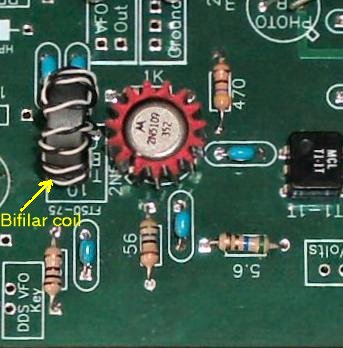
____1 - FT50-75 ferrite core (Bag 4) and wire (Bag 6) ____1 - One of the 8 3/4" Black/White wires Notice below the end of the insulation of the wire overlaps the edge of the core about 1/4". This centers the wire so that both ends have the same amount of insulation over the edge of the core. Wind very tight. |
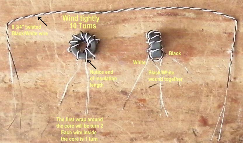
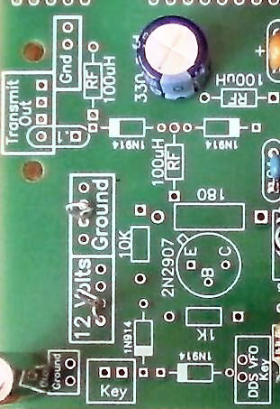
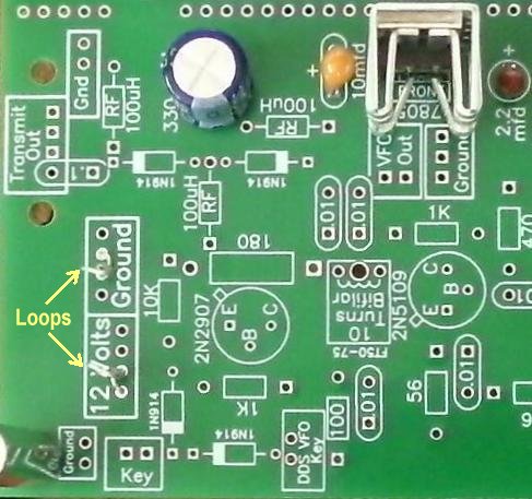
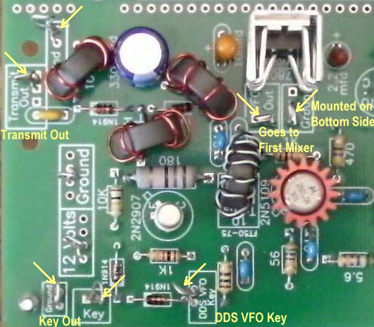
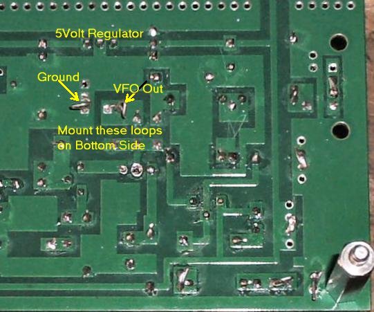
Installing the Wire LoopsThe wire loops for the 'VFO Out' box and 'Ground' are installed underneath the board. The coax cable from the 'VFO Out/Ground' box goes to the First Mixer 'VFO IN/Ground' box. This cable will be installed after the board is populated. |
|
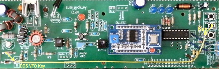
Note: If you built the Arduino DDS VFO for the BLT, go on to Board 1, Section 2. You will not be installing the Key wire as shown below. You have already installed that for the Arduino board. ____1 - Wire Loop, Installed in Key box. Be careful, it is a tight area, don't let the folded over wires on the bottom side touch the adjacent trace.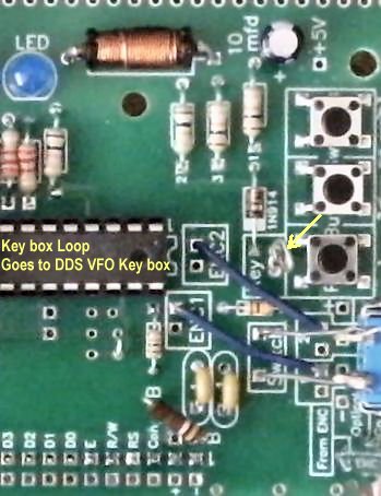 Goes from Key box at Switch 1 to the DDS VFO Key box at the T/R switch circuit. |
|
|
Double Checking Your Work |
|
____Check the dot on the MOSFET and the Minicircuits transformers. |
Send E-Mail || Amateur Radio Receivers || Back to Ham Radio Instructions for the Blue Lightning Transceiver